- 您现在的位置:买卖IC网 > Sheet目录1219 > HIP4082EVAL (Intersil)EVAL BOARD FET DRIVER HIP4082
�� �
�
�Application� Note� 9611�
�inverter.� Ultra-fast� recovery,� 3A� rectifiers� (UF5405),� rectify�
�the� 60kHz� square-wave� voltage� waveform.� Ultra-fast�
�recovery� rectifiers� reduce� the� recovery� energy� dissipated.�
�Even� ultrafast� diodes,� such� as� the� UF5405,� forced� a� slight�
�reduction� in� the� predicted� output� power� rating� of� the� inverter�
�due� to� higher� than� expected� recovery� energy� loss.� Addition�
�of� some� series� impedance� between� the� filter� capacitor,� C� 8� ,�
�and� the� rectifier� bridge,� possibly� even� relocation� of� the� shunt�
�resistor,� R� 23� ,� would� help� to� reduce� this� power.� Users� should�
�keep� this� in� mind� when� designing� their� own� solutions.�
�The� choice� of� square-wave� excitation� waveform� allows� a�
�smaller� rectifier� filter� capacitor� to� be� used,� while� still�
�maintaining� very� low� high� voltage� DC� bus� ripple.�
�The� second� rectifier� provides� control� power� to� the� linear�
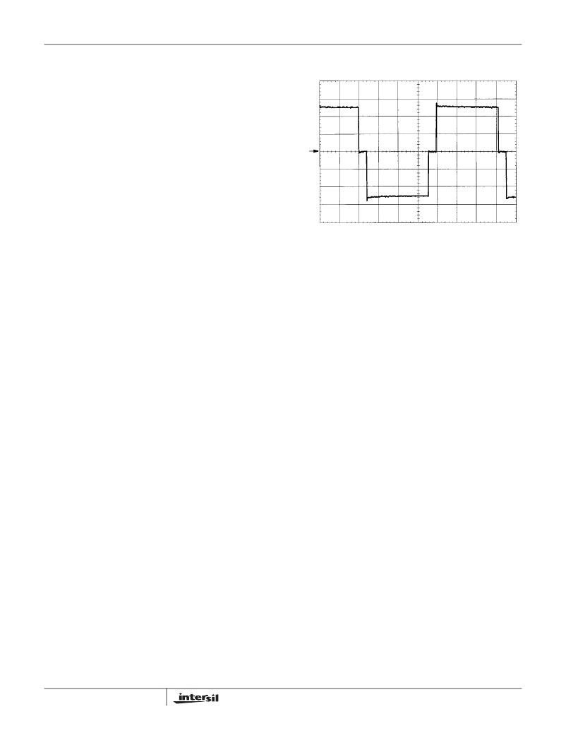
�MOSFET� power� dissipation.� Figure� 3� shows� the� actual�
�output� voltage� waveform.�
�1�
�regulator,� which� in� turn� provides� regulated� 12V� DC� for� all�
�CH1� =� 50V�
�M� =� 2.5� μ� s�
�GLITCH� CH1�
�secondary-side� control� and� gate� drivers.� This� voltage� varies�
�from� 15V� to� 23V� as� the� battery� voltage� varies� from� 10V� to�
�15V.� A� second,� isolated� winding� from� the� transformer� excites�
�this� rectifier.� Unlike� the� high� voltage� rectifier,� this� rectifier�
�bridge� incorporates� 1� ?� of� series� resistance,� R� 35� ,� and� a�
�relatively� small� filter� capacitor,� C� 9� .� No� significant� heating�
�occurred� in� the� 1A� UF4002� rectifiers.� Filter� ripple� is� controlled�
�by� the� linear� regulator,� U� 3� ,� input� (test� point� TP6).� The� low�
�current� linear� regulator� provides� 12V� bias� for� all� of� the�
�secondary-side� control,� driver� ICs,� and� for� MOSFET� gate�
�drive.�
�Secondary-Side� Inverter�
�The� secondary-side� inverter� functions� include� the� power�
�MOSFETs� Q� 6� through� Q� 9� ,� their� associated� gate� resistors�
�and� capacitors,� the� snubber,� the� current-sensing� resistor,� the�
�output� choke,� the� indicator� lamp� and� the� filter.�
�The� inverter� topology� is� a� full-wave� H-bridge� and� synthesizes�
�a� pseudo� sin-wave� by� alternately� switching� on� Q� 6� and� Q� 9� for�
�positive� half� sin-waves� and� Q� 7� and� Q� 8� for� negative� half� sine-�
�waves.� Since� the� inverter� requires� the� ability� to� regulate� the�
�RMS� output� voltage� over� a� wide� ranging� DC� battery� input�
�voltage,� some� means� of� varying� the� conduction� period� of� the�
�Q� 6� -Q� 9� and� Q� 7� -Q� 8� pairs� must� be� implemented.�
�The� choice� of� square-wave� output� over� sine-wave� output�
�simplified� the� pulse-width-modulator� (PWM)� and� minimized�
�FIGURE� 3.� SECONDARY-SIDE� BRIDGE� OUTPUT�
�Varying� the� width� of� the� positive� and� negative� conduction�
�periods� inversely� with� the� voltage� level� of� the� high� voltage�
�bus� maintains� the� RMS� value� of� the� output� waveform�
�relatively� constant.�
�Phase� shifting� two� nearly� perfect� square-waves� from� the� left�
�and� right� half-bridges� making� up� the� inverter� produces� the�
�waveforms� shown� in� Figure� 3.� The� left� half-bridge� includes�
�MOSFETs� Q� 6� and� Q� 8� and� the� right� half-bridge� includes�
�MOSFETs� Q� 7� and� Q� 9� .� The� waveforms� generated� at� the�
�common� connections� (sometimes� referred� to� as� the� phase�
�node� or� phase� terminal)� of� the� MOSFET� half-bridges� appear�
�as� shown� in� Figure� 4.�
�Trace� 1� is� the� voltage� at� the� phase� node� of� Q� 6� and� Q� 8� and�
�Trace� 2� is� the� voltage� at� the� phase� node� of� Q� 7� and� Q� 9� .� The�
�vector� difference� between� the� two� phase� node� voltages� is�
�the� output� voltage� shown� in� Figure� 3.�
�The� required� phase-shift� function� is� implemented� by� a� simple�
�control� circuit.� The� technique� can� be� expanded� to� create�
�sinusoidal� or� other� output� waveform� types� with� added�
�complexity,� of� course.� The� control� circuits� used� in� this� design�
�will� be� discussed� in� the� section,� “Secondary� Inverter� Control�
�Circuits.”�
�The� high� voltage� output� waveform� can� exhibit� a� nasty�
�voltage� transient,� with� the� potential� to� mess� up� the� output�
�voltage� across� the� connected� load� and� to� possibly� destroy�
�the� high� voltage� gate� driver,� HIP2500,� or� the� secondary-side�
�inverter� MOSFETs.� Therefore� phase-to-phase� and� DC� bus�
�snubbers� were� added.� Resistor,� R� 34� and� capacitor,� C� 23� ,�
�implement� the� bus� snubber� and� resistor,� R� 38� and� capacitor,�
�C� 27� ,� comprise� the� phase-to-phase� snubber.� Phase-to-phase�
�or� “AC”� snubbers� allow� their� capacitors� to� completely� charge�
�and� discharge� each� cycle� of� the� switching� waveform� and� at�
�high� switching� frequencies� will� dissipate� a� lot� of� power.� R� 38�
�and� C� 27� were� not� used,� but� space� for� them� was� provided.�
�5�
�发布紧急采购,3分钟左右您将得到回复。
相关PDF资料
HIP4086EVAL
EVALUATION BOARD GP HIP4086
HIP6004EVAL1
EVALUATION BOARD HIP6004
HIP6500BEVAL1
EVALUATION BOARD HIP6500
HIP6501AEVAL1
EVALUATION BOARD ACPI HIP6501
HIP9011EVAL1Z
BOARD EVALUATION FOR HIP9011
HM2H08P115LF
HM2H08P115LF SHROUD STYLE B LF
HM2P12P1LF
HM2 M INS STYLE N WIDE
HM2R06P1LF
MILLIPACS RCP HSG
相关代理商/技术参数
HIP4082IB
功能描述:功率驱动器IC 80V H BRDG FET DRVR RoHS:否 制造商:Micrel 产品:MOSFET Gate Drivers 类型:Low Cost High or Low Side MOSFET Driver 上升时间: 下降时间: 电源电压-最大:30 V 电源电压-最小:2.75 V 电源电流: 最大功率耗散: 最大工作温度:+ 85 C 安装风格:SMD/SMT 封装 / 箱体:SOIC-8 封装:Tube
HIP4082IBS2599
制造商:Intersil Corporation 功能描述:
HIP4082IBT
功能描述:功率驱动器IC TAPE & VER OF STDARD HIP4082IB RoHS:否 制造商:Micrel 产品:MOSFET Gate Drivers 类型:Low Cost High or Low Side MOSFET Driver 上升时间: 下降时间: 电源电压-最大:30 V 电源电压-最小:2.75 V 电源电流: 最大功率耗散: 最大工作温度:+ 85 C 安装风格:SMD/SMT 封装 / 箱体:SOIC-8 封装:Tube
HIP4082IBTS2457
制造商:Intersil Corporation 功能描述:
HIP4082IBZ
功能描述:功率驱动器IC 80V H BRDG FET DRVR RoHS:否 制造商:Micrel 产品:MOSFET Gate Drivers 类型:Low Cost High or Low Side MOSFET Driver 上升时间: 下降时间: 电源电压-最大:30 V 电源电压-最小:2.75 V 电源电流: 最大功率耗散: 最大工作温度:+ 85 C 安装风格:SMD/SMT 封装 / 箱体:SOIC-8 封装:Tube
HIP4082IBZ
制造商:Intersil Corporation 功能描述:IC MOSFET DRIVER QUAD
HIP4082IBZ
制造商:Intersil Corporation 功能描述:MOSFET Driver IC
HIP4082IBZT
功能描述:功率驱动器IC TAPE & VER OF STDARD HIP4082IB RoHS:否 制造商:Micrel 产品:MOSFET Gate Drivers 类型:Low Cost High or Low Side MOSFET Driver 上升时间: 下降时间: 电源电压-最大:30 V 电源电压-最小:2.75 V 电源电流: 最大功率耗散: 最大工作温度:+ 85 C 安装风格:SMD/SMT 封装 / 箱体:SOIC-8 封装:Tube